SPS(Semiconductor Package Substrate)
It is a core part in semiconductor packaging process, which is a high density board of fine circuit that connects semiconductor's electrical signal to the mainboard.
It is used for automotive and various mobile devices that require high reliability.
-
Overview
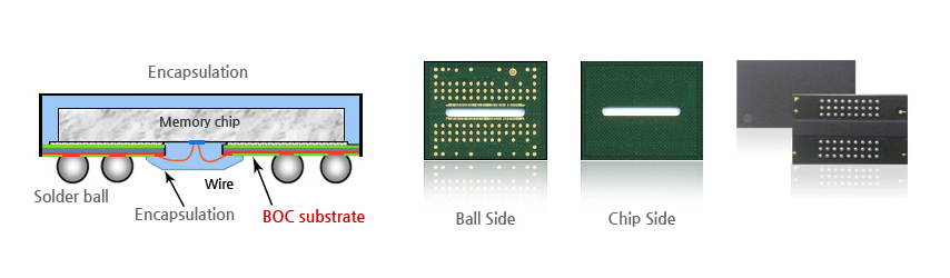
- BOC (Board on Chip)
- BOC is the substrate that connects bonding pad on substrate to the bonding pad of chip by using wire-bonding through the central slot.
- It has the bonding and solder side of the substrate in one plane. It replaced the previous lead frame into laminated substrate, which enables I/O pins to diversify and chip to stack vertically, thus it is widely used in memory chip as it is easy to achieve high speed & high density.
-
Core Technology
- Center pad for wire bonding : Routing Only or Punch Only Process
- Center pad position tolerance
-
Specifications
Items Mass Sample Array Size 240 x 77.5 ㎜ ← Slot Formation Routing or Punch Only ← Slot Size ± 50 µm ± 30 µm PSR Thickness Tolerance 5 µm 4 µm -
Product Image
-
Application
- Desktop & Notebook PC, Server, SSD, Graphic Cards, etc.