SPS(Semiconductor Package Substrate)
It is a core part in semiconductor packaging process, which is a high density board of fine circuit that connects semiconductor's electrical signal to the mainboard.
It is used for automotive and various mobile devices that require high reliability.
-
Overview
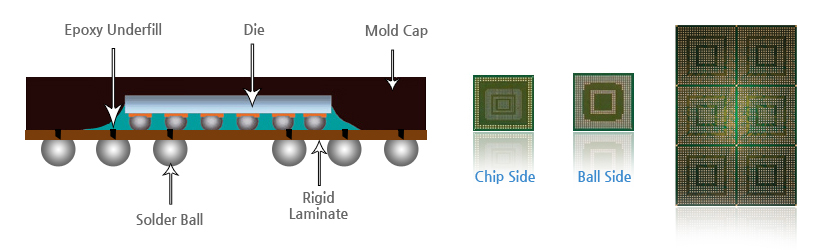
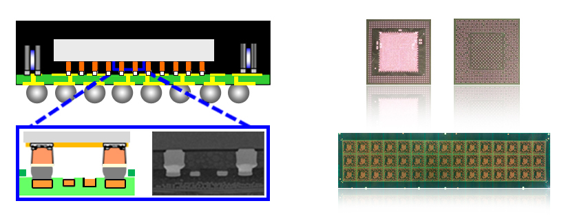
- FC-CSP (Flip Chip CSP)
- FC-CSP is the CSP that connects bumping pad on substrate and bonding pad of Chip in the same location by using flip chip bumping instead of wire-bonding.
It provides the significantly enhanced electrical performance than wire-bonding method and increases chip density with small footprint by removing wire-bonding loop.
Bump formation with below 150µm flip chip bump pitch, bump planarization(coining) technology, fine pattern and surface treatment etc. are our leading core technologies. - ETS (Embedded Trace Substrate)
- ETS provides high density I/O and high reliability by embedding circuit patterns in prepreg(insulation)
It enables MSAP patterning to achieve same or finer pattern than SAP (Line/Space 10/10µm @MSAP).
-
Core Technology
- Fine Pattern formation
- Tight solder resist position tolerance
- Flip Chip Bumping Technology
-
Specifications
Description Mass Development Patterning Trace L/S(@PSAP) 12/12 10/10 & 8/8 Flip Chip Bump Peripheral 40/80 30/60 Area 140,130 120 Solder Position Tol. ± 12.5 ± 10 Surface Treatment Ni/Au+OSP ENEPIG ← -
Product Image
-
FC-CSP (Flip Chip CSP)
-
ETS (Embedded Trace Substrate)
-
-
Application
- PC/Server : DRAM, SRAM
- Smart Mobile Devices : AP, Baseband, Finger print sensor, etc.
- Network : Bluetooth, RF, etc.